Surely, you can try and define human beings in many different ways, but the best way you can do so is by digging into their tendency of getting better on a consistent basis. This tendency, in particular, has really brought the world some huge milestones, with technology emerging as quite a major member of the group. The reason why we hold technology in such a high regard is, by and large, predicated upon its skill-set, which guided us towards a reality that nobody could have ever imagined otherwise. Nevertheless, if we look beyond the surface for one hot second, it will become abundantly clear how the whole runner was also very much inspired from the manner in which we applied those skills across a real world environment. The latter component was, in fact, what gave the creation a spectrum-wide presence, and as a result, initiated a full-blown tech revolution. Of course, the next thing this revolution did was to scale up the human experience through some outright unique avenues, but even after achieving a feat so notable, technology will somehow continue to bring forth the right goods. The same has turned more and more evident in recent times, and assuming one new discovery ends up with the desired impact, it will only put that trend on a higher pedestal moving forward.
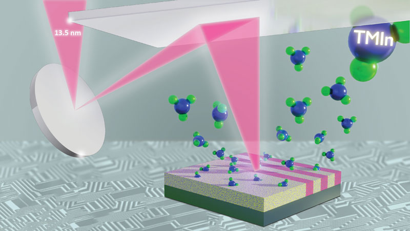
The researching team at US Department of Energy’s Center for Functional Nanomaterials (CFN) has successfully developed a new light-sensitive, organic inorganic hybrid material that enables high-performance patternability by EUV lithography. To understand the significance of such a development, we must start by acknowledging how, with semiconductor feature sizes now approaching only a few nanometers; it has become enormously challenging to sustain this persistent device miniaturization. The stated challenge has got our semiconductor industry to adopt a relatively more powerful fabrication method i.e. extreme ultraviolet (EUV) lithography. In case you are looking for some context, EUV lithography employs light that is only 13.5 nanometers in wavelength to form tiny circuit patterns in a photoresist, the light-sensitive material integral to the lithography process. This photoresist is essentially the template for forming the nanoscale circuit patterns in the silicon semiconductor. However, as we continue our progression towards more advanced but complicated systems, scientists across the globe are now pitted against a challenge of identifying the most effective resist materials. Enter CFN’s latest brainchild. Made from hybrid materials, these new photoresists are composed of both organic materials (those that primarily contain carbon and oxygen atoms) and inorganic materials (those usually based on metallic elements). Furthermore, both parts of the hybrid host their own unique chemical, mechanical, optical, and electrical properties due to their unique chemistry and structures. Hence, upon combining such individually-substantial components, new hybrid organic-inorganic materials are born, materials that boast their own interesting properties. You, the result happens to be a material which is more sensitive to EUV light, meaning it doesn’t need to be exposed to as much EUV light during patterning. Such facility should make a sizeable cut back on process time. Not just that, the new hybrid material also has an improved mechanical and chemical resistance, thus offering a far better value proposition as templates for high-resolution etching.
“To synthesize our new hybrid resist materials, organic polymer materials are infused with inorganic metal oxides by a specialized technique known as vapor-phase infiltration. This method is one of the key areas of materials synthesis expertise at CFN. Compared to conventional chemical synthesis, we can readily generate various compositions of hybrid materials and control their material properties by infusing gaseous inorganic precursors into a solid organic matrix,” said Chang-Yong Nam, a materials scientist at CFN who led the project.
An intriguing detail related to the said development is a change in precursor used for the metal. Rather than banking upon aluminum like they did during previous efforts, the team leveraged indium as an inorganic component. In practice, they made the new resist using a poly (methyl methacrylate) (PMMA) organic thin film as the organic component and infiltrated it with inorganic indium oxide. By doing so, they were able to achieve improved uniformity in subsequent patterning.
That being said, EUV patterning remains a largely inaccessible commodity for now, and that is because of the costs involved.
“It’s currently really hard to do EUV patterning,” said Nam. “The actual patterning machine that industry is using is very, very expensive—the current version is more than $200 million per unit. There are only three to four companies in the world that can use it for actual chip manufacturing. There are a lot of researchers who want to study and develop new photoresist materials but can’t perform EUV patterning to evaluate them. This is one of the key challenges we hope to address.”
In terms of the researching team’s immediate plans with the technology, though, it has already started the work on other hybrid material compositions. The intention is to also make some headway around the processes involved in fabricating them, thus better positioning the industry to pattern smaller, more efficient, and sustainable semiconductor devices.


